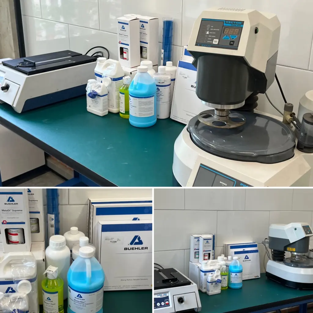
Microsectioning
As the world continues to move towards advanced and sophisticated manufacturing processes, it has become increasingly important to employ techniques that reflect precision and accuracy. Amongst the many techniques used in the field of electromagnetic components, microsectioning has undoubtedly proven to be indispensable. Its widespread usage and high-value application have set it apart as a unique and powerful technique that guarantees quality assurance in modern manufacturing practices.
The process involves testing and evaluating small samples of printed circuit boards (PCBs), printed circuit assemblies (PCAs) or Crimp Connections (cables and wires) which is commonly known as cross-sectioning or metallographic preparation. To achieve optimal results, a small part of the sample is destroyed to examine the cut surfaces meticulously. This allows engineers and technicians to effectively scrutinize the standard and reliability of a particular product, ensuring that it meets with industry standards.
It wouldn’t be feasible to ensure the quality and reliability of PCBs, PCAs and Crimp Connections without the aid of microsectioning; a process that has become the hallmark of dependable and trustworthy manufacturing practices. Its use is, therefore, essential in guaranteeing reliable production and quality control. In sum, microsectioning remains an essential tool for modern manufacturing practices, one that enables the production of efficient, reliable, and high-standard products.
Typically, Microsectioning Analysis can help to check the quality of:
- The base material of the PCB
- Build checking in multi-layer boards
- Hole-wall plating thickness in a plated through hole
- Thickness of external and internal conductors
- Registration of external and internal pads
- Connection between layers
- Thickness of Surface Finish
- Thickness of Soldermask or Coverlay
- Solder wetting
- Solder porosity
- Solder meniscus
- Lead-to-pad geometry
- Lead-to-pad solder thickness
- Lifted leads and other flaws caused by soldering process stresses
- Unacceptable solder microstructure
- Proper crimp geometry (width / Height)
- Conductor wire compression
As a laboratory service provider, we offer micrograph analyses and microscopic images of electronic assemblies, crimp connections, joints and through-hole vias, among others.